ELECTRICAL TECHNOLOGY (ELECTRONICS) GRADE 12 MEMORANDUM - NSC EXAMS PAST PAPERS AND MEMOS MAY/JUNE 2021
Share via Whatsapp Join our WhatsApp Group Join our Telegram GroupELECTRICAL TECHNOLOGY (ELECTRONICS)
GRADE 12
NATIONAL SENIOR CERTIFICATE EXAMINATIONS
MAY/JUNE 2021
INSTRUCTIONS TO THE MARKERS
- All questions with multiple answers imply that any relevant, acceptable answer should be considered.
- Calculations:
2.1 All calculations must show the formulae.
2.2 Substitution of values must be done correctly.
2.3 All answers MUST contain the correct unit to be considered.
2.4 Alternative methods must be considered, provided that the correct answer is obtained.
2.5 Where an incorrect answer could be carried over to the next step, the first answer will be deemed incorrect. However, should the incorrect answer be carried over correctly, the marker has to re-calculate the values, using the incorrect answer from the first calculation. If correctly used, the candidate should receive the full marks for subsequent calculations. - This memorandum is only a guide with model answers. Alternative interpretations must be considered and marked on merit. However, this principle should be applied consistently throughout the marking session at ALL marking centres.
QUESTION 1: OCCUPATIONAL HEALTH AND SAFETY
1.1 'Safe' means free from any hazard. ✓ (1)
1.2
Discipline. ✓
Sense of teamwork. ✓
Emphasis on quality.
Integrity.
Sense of responsibility. (2)
1.3
The use of power tools. ✓
The handling of hand tools.
The use of etching acid and other chemicals. (1)
1.4
Poor ventilation reduces the correct amount of oxygen ✓ which might lead to drowsiness. ✓
Covid-19 protocols also refer to proper ventilation that must be adhered to. (2)
1.5
To take reasonable care for the health and safety of himself/herself and others who may be affected by his/her act. ✓
Cooperate with the employer or persons to enable that any duty given by the employer to the employee shall be performed or complied with according to the requirements and procedures. ✓ (2)
1.6 Human rights ensure human dignity ✓ and that people are treated with respect and not exploited. ✓ (2)
[10]
QUESTION 2: RLC CIRCUITS
2.1
2.1.1 Phase angle is the shift in phase between the supply voltage ✓ and the current ✓ in a circuit which contain reactances and resistances. (2)
2.1.2 Capacitance is the ability of a capacitor to store an electric charge.✓ (1)
2.2
It will affect the phase angle. ✓
It will oppose the current flow in the circuit. ✓
Lenz’s law states that when alternating current flows through an inductor, a back emf is set up which is opposite to the applied voltage. (2)
2.3
2.3.1
XL = 2 x π x f x L
= 2 x π x 60 x 300 x 10-3
= 113,10Ω
(3)
2.3.2
Z = √R2 + (XL - XC)2
= √302 + (113,10 - 30,32)2
= 88,05 Ω
(3)
2.3.3 Inductive circuit. ✓ The inductive reactance is greater than the capacitive reactance. ✓ (2)
2.4
2.4.1
![]()
=300/50
=6A(3)
2.4.2
![]()
=300/3
=100Ω
(3)
2.4.3
IT= √IR2 + (IL-IC)2
= √42 + (3-6)2
=5A
(3)
2.4.4
![]()
=Cos-1 4/5
=36,87
(3)
2.5
2.5.1 Impedance. ✓ (1)
2.5.2 Capacitive reactance is greater ✓ than the inductive reactance.✓ (2)
2.5.3
The inductive reactance is represented by a straight line because it is directly proportional to the frequency ✓ of the supply voltage and the capacitive reactance is represented by the curved line because it is indirectly proportional to the frequency of the supplied voltage.✓
The Reactance value of a capacitor has a very high value at low frequencies but quickly decreases as the frequency across it increases. (2)
2.5.4
fr = 1
2π√LC
= 1
2π √2,12 x 1,47 x 10-6
= 90,16 Hz
(3)
2.5.5
Tuning circuits. ✓
Radio circuits.
Oscillator circuits.
TV circuits.
Filter circuits.
Band pass filter. (1)
2.6
2.6.1 The higher the value of the Q-factor the greater the value of the current flow.✓ (1)
2.6.2
Half power points are the upper and lower cut off frequencies in a circuit.✓
Point at which the output power has dropped to half of its peak value, at a level of approximately -3db. (1)
2.6.3
- The value of the series resistor.✓
- The inductor/capacitor (L/C) ratio. ✓ (2)
2.6.4 As the Q factor of the circuit is lowered, its selectivity decreases✓ and its bandwidth increases.✓ (2)
[40]
QUESTION 3: SEMICONDUCTOR DEVICES
3.1
MOSFET✓
JFET (1)
3.2
3.2.1 Enhancement-mode ✓ N-channel ✓ MOSFET (2)
3.2.2
Switch.✓
Used in linear voltage regulator circuits.
Used in inverters. (1)
3.3
3.3.1
Y = Negative resistance region ✓
Z = Saturation region ✓ (2)
3.3.2 The valley point ✓ (1)
3.3.3 When the voltage across the emitter is increased✓ from zero to point B the critical voltage point✓, the reverse leakage current decreases to the point that no current flows in either direction. ✓ (3)
3.4
Infinite gain.✓
Infinite input impedance.✓
Zero output impedance.✓
Infinite Bandwidth.✓
Infinite common mode rejection ratio.
Unconditional stability. (4)
3.5
3.5.1
=1 + 50000/10000
=6
(3)
3.5.2![]()
=1,5 x (1 + 50000/10000)
=9V
(3)
3.5.3 If the value of the feedback resistor is decreased the gain of the amplifier will decrease✓ causing the output voltage to decrease. ✓ (2)
3.6
3.6.1 Pin 2 = Trigger input.✓ (1)
3.6.2 This pin sets the voltage at which the 555 IC will trigger. It is used to maintain ✓ the voltage across the timing capacitor ✓ which is discharged through pin 7. ✓ (3)
3.6.3 The 555 IC can operate from power supply voltages of between +5 V ✓ and +18 V. ✓ (2)
3.6.4 In this mode the 555 timer is astable ('free running'), therefore its output will continuously toggle between High and Low ✓ thus generating a continuous train of square-wave pulses. ✓ (2)
QUESTION 4: SWITCHING CIRCUITS
4.1
4.1.1 Bistable multivibrator.✓ (1)
4.1.2 A positive pulse.✓ (1)
4.1.3 The 741 Op-amp acts as a comparator ✓ that compares the two voltages on its input.
It acts as an amplifier ✓ for the input signals that drives the output to one of its saturation states. (2)
4.1.4 LED1 (red). ✓ (1)
4.1.5 Positive. ✓ (1)
4.2
4.2.1 +9 V. ✓ (1)
4.2.2 0 V. ✓ (1)
4.2.3 The circuit output will change state only when a trigger pulse greater than –Vref ✓ is applied to the inverting input.✓ (2)
4.2.4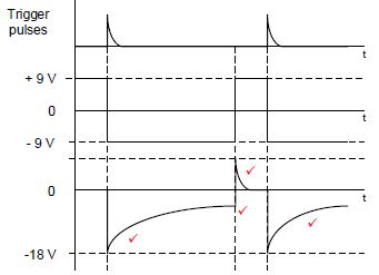
4.3
4.3.1 R1 & R2. ✓ (1)
4.3.2 The output will keep on oscillating between high and low states because both the trigger pin 2 and threshold pin 6 ✓ is connected to the top of the timing capacitor. ✓ (2)
4.3.3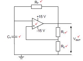
NOTE: The circuit connection must be correct before allocatingmarks to components.
The supplies should be indicated for the Op-amp to be accepted as correct. (6)
4.4
- The signal is fed into the inverting input of the Op-amp which acts as a comparator, comparing the voltages on its two input terminals. ✓
- The difference on the two input terminals drives the output of the Op-amp into one of its saturation states. ✓
- This output is divided across the two resistors RF and R1 into a fraction which is fed back to the non-inverting input. ✓
- The voltage on the non-inverting input determines (sets) the lower and upper trigger voltage levels. ✓
- The voltage on the inverting input is compared to the voltage on the noninverting input (trigger voltage level), if it’s lower than the trigger voltage
level, the output is driven into positive saturation. ✓ - If it is higher than the trigger voltage, it is driven into negative saturation.✓
(6)
4.5
4.5.1 A summing amplifier is used to add two or more different input signals ✓ to create one amplified output signal. ✓ (2)
4.5.2 VOUT=-(V₁+V₂+V₃)
=-(0,5+1,2+0,9)
=-2,6v
OR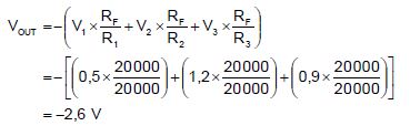
4.5.3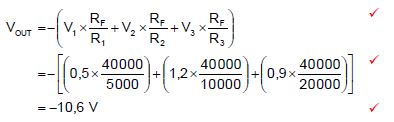
4.5.4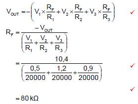
OR
RF=AV x RIN
=4 x 20000
=80000Ω
=80kΩ
NOTE: A resistance cannot be negative, that is the reason why the negative sign is omitted in the substitution stage. The negative sign only shows inversion of the output signal.
4.5.5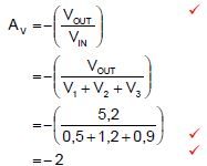
(3)
4.6
4.6.1
A – Passive RC differentiator. ✓
B – Passive RC integrator. ✓ (2)
4.6.2
With a long time constant the left hand plate of the capacitor immediately charges up to positive potential, ✓ thereafter the right hand plate slowly discharges ✓ and before it is completely discharged the polarity of the input swings to the opposite potential.✓ The capacitor then immediately charges to negative potential again and the process repeats itself. (3)
4.6.3
To convert ✓ square waves into triangular waves ✓
To change the shape of one type of wave to another wave. (2)
4.7
4.7.1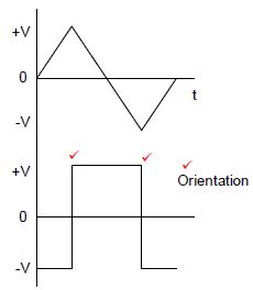
NOTE: The trigger points are only accepted if the wave shape is
correct.
1 mark for correct orientation if the wave shape is correct (3)
4.7.2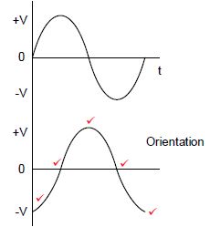
NOTE: The trigger points are only accepted if the wave shape is
correct.
1 mark for correct orientation if the wave shape is correct (5)
4.7.3
- The input and output impedance is improved✓
- Gain is boosted ✓
- Circuit is more stable. (2)
[60]
QUESTION 5: AMPLIFIERS
5.1
5.1.1 When the circuit reduces the output amplitude ✓ of the signal power between its input and output. ✓ (2)
5.1.2 A circuit that allows higher frequencies to pass ✓ and attenuates (reduces) lower frequencies ✓ than the pass frequency (2)
5.2
5.2.1 A small signal amplifier is used to enlarge a very low-level signal ✓ of voltage or current to a more manageable size. ✓ It has a high gain. (2)
5.2.2 A power amplifier takes the larger signal at its input ✓ and boosts it to a sufficiently large level as to drive a loudspeaker. ✓ The gain is typically low (2)
5.3.
5.3.1
- To predict the output voltage and output current variations for a specified base current. ✓
- Find the current gain of the amplifier.
- Predict the amplifier performance. (1)
5.3.2 The three DC load lines have different Collector Resistor (RC)values ✓ resulting in three different values of collector current (IC)✓ whilst the supply voltage remains constant. ✓
NOTE: If the learner simply reads the information from the graph and it is correct, 1 mark is awarded. The learner needs to indicate knowledge or the RC resistor value that influences the IC current if the supply voltage remains constant. Then only the other two marks will be awarded. (3)
5.3.3
= 12
3 x 10-3
=kΩ
(3)
5.4 The amplifier amplifies the full cycle ✓ of the input signal with a conduction angle of 360 degrees. ✓ (2)
5.5 'Infinite bandwidth' occurs when all frequencies pass through the circuit without attenuation.✓ (1)
5.6
5.6.1 Amplifier ✓ with a closed loop feedback / negative feedback. (1)
5.6.2
The bandwidth will decrease. ✓
The gain will increase. ✓
Distortion may increase. ✓
The amplifier will become unstable (3)
5.7
5.7.1 Transformer coupled amplifier circuit.✓ (1)
5.7.2
- At lower frequencies, the XC of the coupling capacitor is high, reducing the gain of the amplifier. ✓
- Between Fco1 and Fco2, the amplifier operates linearly and the gain remains uniform. ✓
- At Q1 and Q2, the transformer coupling oscillates with the capacitive coupling and the gain increases. ✓
- Above resonance, XC increases and the gain decreases. ✓ (4)
5.8
5.8.1 A. ✓ (1)
5.8.2 D. ✓ (1)
5.8.3 C. ✓ (1)
5.8.4 B. ✓ (1)
5.9
5.9.1 Amplifiers require a DC voltage to provide a constant power source ✓ which the amplifier can in turn use to amplify the AC input signal. ✓ (2)
5.9.2 Cross-over distortion.✓ (1)
5.9.3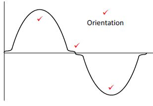
NOTE:
2 marks (1 for each correct half-cycle)
1 mark for the distortion
1 mark for correct orientation if the wave shape is correct (4)
5.9.4
- The NPN transistor (Q1) will amplify only the positive half of the input cycle to it ✓ whereas the PNP transistor (Q2) will only amplify the negative half of the input cycle to it.✓
- These two halves are then combined to give an output.✓
- Resistors RB1 and RB2 are acting as input current limiting resistors to the base of the transistors. ✓
- The output waveform will be much larger because two transistors are amplifying the input signal.✓
(5)
5.10
5.10.1 Class C amplification.✓ (1)
5.10.2 Radio Frequency Amplifier is a selective amplifier ✓ capable of amplifying only a single high frequency ✓ or frequency to be picked up by the receiver ✓ and to suppress all other frequencies. (3)
5.10.3 The unwanted frequencies (noise) are the frequencies that are not amplified ✓ or are rejected by the radio frequency amplifier. (1)
5.10.4 To resonate at the required frequency ✓ and suppress the unwanted frequencies. ✓ (2)
5.10.5 The resonating frequency of the circuit can be varied by adjusting ✓ the value of the variable capacitor. ✓ (2)
5.10.6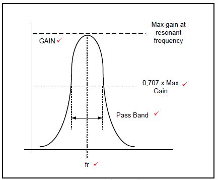
(4)
NOTE: A maximum of 4 marks is allowed for this question.
5.11 When the circuit is switched 'ON' capacitor C3 will start charging due to the voltage across the collector. ✓ There will be a voltage across L1 and L2, which appears in an inverted form. ✓ This voltage will drive the transistor Q1 base voltage in the opposite direction, thereby switching it OFF. ✓ C3 will discharge through L1 and L2, and push the tank circuit into oscillation. ✓ (4)
[60]
TOTAL: 200