Electrical Technology: Digital Grade 12 Questions - NSC Exams Past Papers and Memos September 2019 Preparatory Examinations
Share via Whatsapp Join our WhatsApp Group Join our Telegram GroupINSTRUCTIONS AND INFORMATION
- This question paper consists of FIVE questions.
- Sketches and diagrams must be large, neat and fully labelled.
- Show ALL calculations and round off answers to TWO decimal places. Show the units for ALL answers and calculations.
- Number the answers correctly according to the numbering system used in this question paper.
- You may use a non-programmable calculator.
- A formula sheet is provided at the end of this question paper.
- Write neatly and legibly.
QUESTIONS
QUESTION 1: OCCUPATIONAL HEALTH AND SAFETY (GENERIC)
1.1 Name THREE unsafe conditions that cause most accidents in the workshop. (3)
1.2 Explain the purpose of the Occupational Health and Safety Act. (2)
1.3 Give TWO unsafe acts in a school workshop that can cause an accident. (2)
1.4 Describe THREE standard treatments for electric shock after the electricity has been removed. (3) [10]
QUESTION 2: SWITCHING CIRCUITS (GENERIC)
2.1 With reference to FIGURE 2.1, answer the following questions.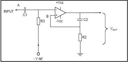
FIGURE 2.1: MULTIVIBRATOR
2.1.1 Identify the multivibrator in FIGURE 2.1. (1)
2.1.2 Name TWO characteristics of this multivibrator. (2)
2.1.3 Explain the function of the network C2 and R2. (3)
2.1.4 Analyse FIGURE 2.1 above and explain the THREE ways to change this circuit in order to have a variable time in the high state. (4)
2.1.5 Explain the principle of operation of the circuit in FIGURE 2.1. (8)
2.1.6 Name ONE application of this multivibrator. (1)
2.2 With reference to FIGURE 2.2, answer the following questions. 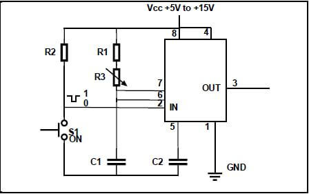
FIGURE 2.2: MULTIVIBRATOR
2.2.1 Explain the function of R1 in the circuit. (2)
2.2.2 Name TWO methods to vary the time period of this circuit. (2)
2.2.3 Explain the effect on the output waveform if R3 is changed from 10 kΩ to 27 kΩ. (1)
2.3 Draw a fully labelled circuit diagram of an Op-Amp Astable multivibrator circuit. (8)
2.4 Draw a fully labelled hysteresis characteristic curve with reference to the Schmitt trigger. (6)
2.5 Define the term hysteresis with reference to the Schmitt trigger. (2)
2.6 Name TWO applications of a Schmitt trigger. (2)
2.7 Draw a fully labelled circuit diagram of a temperature sensor circuit. (8)
2.8 Draw a fully labelled circuit diagram of a summing amplifier with three inputs. (6)
2.9 A summing amplifier has three input resistors with the following values:
R1 = 30 kΩ, R2 = 17 kΩ, R3 = 21 kΩ. The output voltage for this circuit is given as -2,7 V. The known input voltages are: V1 = 150 mV, V2 = 430 mV.
Calculate the value of V3 if this circuit has a 120 kΩ feedback resistor. (4) [60]
QUESTION 3: SEMICONDUCTOR DEVICES (SPECIFIC)
3.1 State the THREE stages of a 741 Op-Amp. (3)
3.2 Explain the term Common Mode Rejection Ratio. (2)
3.3 With reference to FIGURE 3.3 below, answer the following questions. 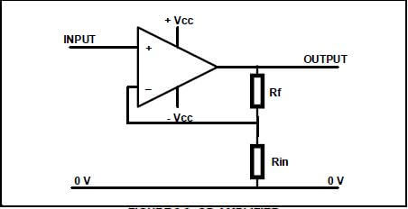
FIGURE 3.3: OP-AMPLIFIER
3.3.1 Identify the Op-Amplifier in FIGURE 3.3. (1)
3.3.2 Calculate the gain of the amplifier if the feedback resistor has a value of 1 kΩ and the input resistor has a value of 1 900 Ω. (2)
3.4 Name THREE uses for the 555 timer IC. (3)
3.5 Name TWO operating boundaries of a 555 timer IC. (2)
3.6 Explain why this IC is called a 555 timer IC. (3)
3.7 With reference to FIGURE 3.7 below, label pin 6.
3.7.1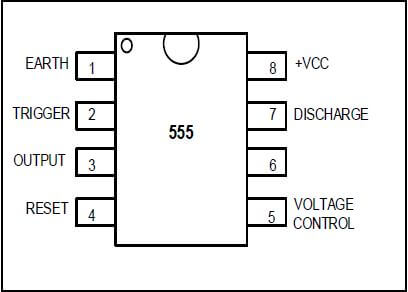
FIGURE 3.7: 555 TIMER (1)
3.7.2 With reference to a 555 timer IC, explain the function of pin 2 (trigger). (3) [20]
QUESTION 4: DIGITAL AND SEQUENTIAL DEVICES (SPECIFIC)
4.1 Explain the term common anode with reference to the seven segment LED display. (2)
4.2 Draw a fully labelled circuit diagram of a sinking digital output. (4)
4.3 Explain the term polarisation of light with reference to LCD displays. (3)
4.4 With reference to FIGURE 4.1 below, answer the questions to follow.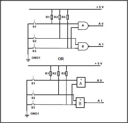
FIGURE 4.4: LOGIC CIRCUIT
4.4.1 Identify the circuit in FIGURE 4.4. (1)
4.4.2 Draw a truth table for the circuit in FIGURE 4.4. (5)
4.4.3 Explain the function of the circuit in FIGURE 4.4. (2)
4.5 Draw the logic symbol for a half adder. (2)
4.6 With reference to FIGURE 4.6 below, answer the questions to follow. 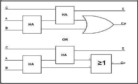
FIGURE 4.6: LOGIC CIRCUIT
4.6.1 Identify the circuit in FIGURE 4.6. (1)
4.6.2 Draw the fully labelled logic diagram for the logic circuit in FIGURE 4.6 using AND gates, EXCLUSIVE OR and OR gates. (8)
4.7 Draw a fully labelled logic circuit of an active high latch (RS Latch). (3)
4.8 Complete the truth table below for an active high latch.
MODE OF OPERATION INPUTS | INPUTS | OUTPUTS | ||
ILLEGAL | S | R | Q1 | Q2 |
0 | 0 | |||
SET | 0 | 1 | ||
RESET | 1 | 0 | ||
HOLD | 1 | 1 | ||
(4)
4.9 Draw a fully labelled circuit diagram of a D Latch flip-flop using NAND gates, EXCLUSIVE OR gates and INVERTER. (8)
4.10 Explain the term positive edge triggering. (2)
Copyright reserved Please turn over
10 ELECTRICAL TECHNOLOGY: DIGITAL (EC/SEPTEMBER 2019)
4.11 With reference to FIGURE 4.11 below, explain the principle of operation of an up/down counter.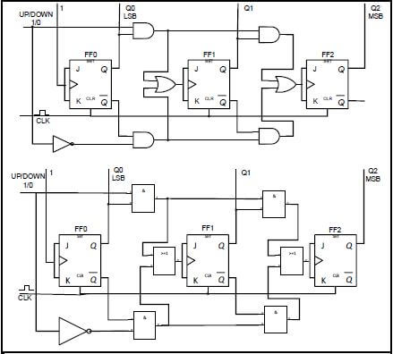
(8)
FIGURE 4.11: UP / DOWN COUNTER
4.12 Explain the term truncated counter. (2) [55]
QUESTION 5: MICROCONTROLLERS (SPECIFIC)
5.1 Give the definition of a microcontroller. (3)
5.2 Name TWO uses of microcontrollers as used in day-to-day life devices. (2)
5.3 Name the main disadvantage of a microcontroller. (2)
5.4 With reference to the parts of a microcontroller, answer the questions that follow:
5.4.1 Define the Central Processing Unit (CPU). (2)
5.4.2 Describe the function of the Input/Output interface (I/O). (2)
5.5 Briefly define integrated logic. (1)
5.6 Explain the function of each of the following registers with reference to the Central Processing Unit (CPU):
5.6.1 Program counter (3)
5.6.2 Memory data register (1)
5.7 Discuss the Random Access Memory (RAM) with reference to the CPU of a microcontroller. (5)
5.8 With reference to communication in a microcontroller, state the THREE BUSSES that the system bus consists of. (3)
5.9 Define communication protocol as an element in a microcontroller. (2)
5.10 Explain the differences between simplex communication and duplex communication by means of fully labelled block diagrams. (6)
5.11 Name TWO advantages of asynchronous communication. (2)
5.12 Draw a fully labelled block diagram of an 8-bit serial communication system. (7)
5.13 With reference to communication peripherals, name TWO advantages of the Serial Peripheral Interface (SPI). (2)
5.14 Identify the following flow diagram symbols.
5.14.1  (1)
(1)
5.14.2  (1)
(1)
5.15 Draw a flow diagram for a mono stable device that has only one stable state. The program switches the output on and off every 5 seconds and then returns to the original state. (10) [55]
TOTAL: 200
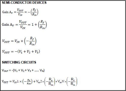
FORMULA SHEET - DIGITAL