Electrical Technology: Electronics Questions - Grade 12 September 2021 Preparatory Exams
Share via Whatsapp Join our WhatsApp Group Join our Telegram GroupINSTRUCTIONS AND INFORMATION
- This question paper consists of SIX questions.
- Sketches and diagrams must be large, neat and FULLY LABELLED.
- Show ALL calculations and round off answers to TWO decimal places.
- Number the answers correctly according to the numbering system used in this question paper.
- You may use a non-programmable calculator.
- Show the units for ALL answers of calculations.
- A formula sheet is attached at the end of this question paper.
- Write neatly and legibly.
QUESTIONS
QUESTION 1: MULTIPLE CHOICE QUESTIONS
Various options are provided as possible answer to the following questions. Choose the answer and write only the letter (A–D) next to the question numbers (1.1 to 1.15) in the ANSWER BOOK, for example 1.16 A.
1.1 To prevent infection when treating burns, the following should NOT be done:
- Do not take a pain killer
- Do not pop blisters
- Do not use a sterile gauze or bandage
- Do not hold the burned area under cool running water (1)
1.2 In a purely capacitive circuit, the relationship between the voltage and current is as follows:
- The current leads the voltage
- The current lags the voltage
- The current and voltage are in phase
- The current is zero (1)
1.3 During resonance the …
- inductive reactance is greater than capacitive reactance.
- capacitive reactance is greater than inductive reactance.
- impedance is equal to 1.
- inductive reactance is equal to capacitive reactance. (1)
1.4 In a 240 V, 50 Hz RCL circuit with an inductance of 50 mH, the inductive reactance is equal to …
- 151,7 Ω.
- 151,7 H.
- 15,71 Ω.
- 15,71 H. (1)
1.5 Which TWO characteristics are of interest in a JFET?
- Transfer and output
- UJT and output
- N-channel and transfer
- Darlington pair and metal oxide silicon field effect transistor (1)
1.6 Which device relies on the creation of an electric field within its body to control current flow?
- Field effect transistor
- Amplifier
- Gain
- 555 timers (1)
1.7 The maximum current a 555 IC can either sink or source is:
- 2 A
- 200 A
- 2 m A
- 20 m A (1)
1.8 With reference to a monostable multivibrator, the time an output stays high, is determined by:
- The time constant (RC)
- The length of time you push the button
- The magnitude of the supply voltage
- It will stay high indefinitely (1)
1.9 The Bistable multivibrator has the following characteristics:
- Free running with ONE input
- Free running with TWO inputs
- TWO stable states with TWO inputs
- NO stable states with ONE input (1)
1.10 A Light Dependant Resistor (LDR) will change value due to:
- Wind blowing on the LDR
- Current flowing through the LDR
- A voltage drop across the LDR
- The change of light shining on the LDR (1)
1.11 The output waveform of a Schmitt trigger circuit will always be a:
- Sine wave
- Triangular wave
- Radio wave
- Square wave (1)
1.12 Which ONE is the application of a RC coupled amplifier?
- Radio or TV receivers
- Most use in impedance matching
- Used as a driver amplifiers
- Output amplifiers (1)
1.13 A disadvantage of a RC coupled amplifier is …
- RF communication.
- that it is unsuitable for low frequency amplification.
- optical fibre communications.
- offers a constant gain over a wide frequency band. (1)
1.1.4 The … of an amplifier is the range of frequencies within which the gain does not fall below 0,7 of its maximum value.
- complimentary push pull
- transistor
- bandwidth
- radio frequency amplifier (1)
1.15 Which ONE is an important area on the frequency response curve?
- Impedance matching
- Low frequency cut off region
- Negative feedback
- De isolation (1)
[15]
QUESTION 2: OCCUPATIONAL HEALTH AND SAFETY
2.1 Give the meaning of the following with reference to the Occupational Health and Safety, 1993 (Act 85 of 1993).
2.1.1 Risk (1)
2.1.2 Safe (1)
2.2 Explain the difference between quantitative risk analysis and qualitative risk analysis. (5)
2.3 State ONE example of a dangerous practice in an electrical workshop. (1)
2.4 Explain how inadequate lighting is an unsafe condition. (2)
[10]
QUESTION 3: RLC CIRCUITS
3.1 Draw a neat, labelled characteristic curve showing the relationship between the inductive reactance and the frequency in a pure inductive circuit. (2)
3.2 State the relationship between the capacitive reactance and the frequency in a pure capacitive circuit. (1)
3.3 Define the term phase angle with reference to RLC circuits. (2)
3.4 FIGURE 3.4 below shows the phasor diagram of the voltages and current in a series circuit. Answer the questions that follow.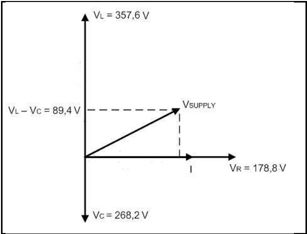
FIGURE 3.4
3.4.1 State with reference to the current, whether the phase angle is leading or lagging. (1)
3.4.2 Calculate the value of the supply voltage. (3)
3.4.3 Explain when the current would be in phase with the voltage of the circuit. (2)
3.5 State where resonant circuits are used. (1)
3.6 Describe the differences between the characteristics of series and parallel resonance. (2)
3.7 The series RLC circuit in FIGURE 3.7 consists of a 22 Ω resistor, an inductor of 50 mH and a capacitor with a reactance of 42,44 Ω. The series combination is connected to a 110 V/50 Hz supply. Answer the questions that follow.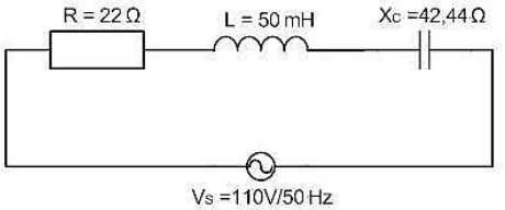
FIGURE 3.7
Given:
- R = 22 Ω
- L = 50 Mh
- X? = 42,44 Ω
- VS = 110 V
- f = 50 Hz
Calculate:
3.7.1 The inductive reactance (3)
3.7.2 The impedance of the circuit (3)
3.7.3 The value of the capacitor in the circuit in micro-farad (4)
3.8 Refer to FIGURE 3.8 below and answer the questions that follow.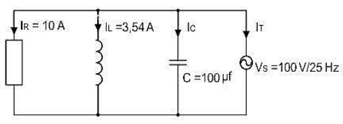
FIGURE 3.8
Given:
- IR = 10 A
- IL = 3,54 A
- C = 100 µF
- VS = 100 V
- f = 25 Hz
Calculate:
3.8.1 The current flowing through the capacitor (5)
3.8.2 The total current flowing through the circuit (3)
3.8.3 The phase angle (3)
[35]
QUESTION 4: SEMICONDUCTOR DEVICES
4.1 Name TWO types of junction field effect transistors. (2)
4.2 List THREE operating regions of the UJT. (3)
4.3 Draw a fully labelled symbol of the N-channel JFET. (3)
4.4 Refer to FIGURE 4.4 below and answer the questions that follow.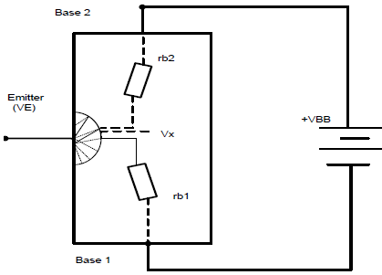
FIGURE 4.4: UJT
4.4.1 State the type of material used to produce the substrate. (2)
4.4.2 Explain how the intrinsic standoff ratio is determined. (2)
4.4.3 Explain what happens when the voltage on the emitter terminal (VE) is increased above Vx. (2)
4.5 Draw a fully labelled symbol of a Darlington pair transistor. (3)
4.6 Describe TWO advantages of a Darlington pair. (4)
4.7 Refer to FIGURE 4.7 and answer the questions that follow.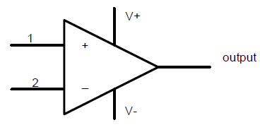
FIGURE 4.7: OP-AMP SYMBOL
4.7.1 Label number 1 and 2. (2)
4.7.2 Explain why the op-amp uses a dual voltage supply. (2)
4.8 Name the THREE stages of an op-amp. (3)
4.9 Identify Pin 7 of a 741 op-amp. (1)
4.10 With reference to op-amp characteristics, explain the term bandwidth. (4)
4.11 Explain why an op-amp as a voltage follower is an ideal coupling stage (buffer) between two unevenly matched stages. (2)
4.12 With reference to 555 IC, explain the function of pin 5 (control voltage). (4)
4.13 Explain the function of using a small value capacitor connected from pin 5 to ground on a 555 IC. (2)
4.14 Name the TWO primary building blocks of a 555 IC. (2)
4.15 Name TWO modes the 555 IC is set up to function in. (2)
[45]
QUESTION 5: SWITCHING CIRCUITS
5.1 With reference to FIGURE 5.1 below, answer the following questions.
FIGURE 5.1: MULTIVIBRATOR
5.1.1 Identify the circuit in FIGURE 5.1 above. (1)
5.1.2 State the function of R3. (1)
5.1.3 Describe what happens when the RESET switch, S2 is pressed. (3)
5.1.4 Explain the purpose of C1 which is connected to ground from pin 5. (3)
5.1.5 Explain what the effect would be on the circuit if R1 and R2 were not added to the circuit. (2)
5.2 Draw a fully labelled circuit diagram for a monostable multivibrator op-amp circuit. (6)
5.3 Explain how you would vary the length of time that a monostable multivibrator circuit output stays ‘HIGH’. (3)
5.4 Explain how to eliminate switch bounce. (1)
5.5 Draw a fully labelled circuit diagram for a temperature sensor using a 741 op-amp. (8)
5.6 Explain the principle of operation of a Light Dependant Resistor (LDR). (4)
5.7 Refer to FIGURE 5.7 below and answer the questions that follow.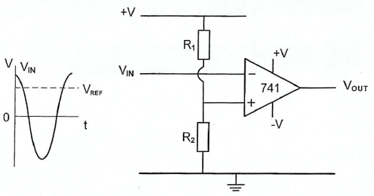
FIGURE 5.7: COMPARATOR
5.7.1 Explain what is meant with open loop with reference to FIGURE 5.7. (2)
5.7.2 Describe the principle of operation of a comparator. (6)
5.8 Refer to FIGURE 5.8 below and answer the questions that follow.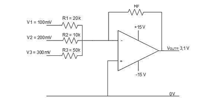
FIGURE 5.8: SUMMING AMPLIFIER
5.8.1 State how an input signal can be added to the summing amplifier. (1)
5.8.2 Calculate the value of the feedback resistor (RF). (4)
5.8.3 State why the output voltage is negative in FIGURE 5.8. (1)
5.9 Draw the circuit diagram for a passive integrator. (4)
[50]
QUESTION 6: AMPLIFIERS
6.1 Refer to FIGURE 6.1 below and answer the following questions.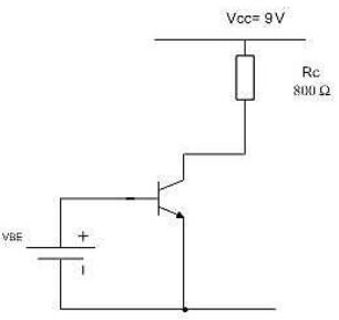
FIGURE 6.1
6.1.1 List TWO reasons for biasing a transistor. (2)
6.1.2 Describe the term Q-point on a DC load line. (2)
6.1.3 State the formula for Vce. (1)
6.1.4 Calculate the maximum collector current. (3)
6.1.5 Draw the DC load line and indicate the maximum current and Vce. (3)
6.2 Audio amplifiers terminal currents are measured as 3,6 mA input current and 15,3 mA output current. Calculate the amplifier current in decibels. (3)
6.3 Explain TWO advantages of negative feedback. (2)
6.4 Refer to FIGURE 6.4 below and answer the questions that follow.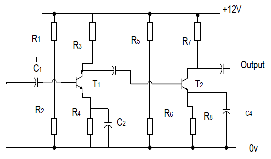
FIGURE 6.4: RC COUPLED AMPLIFIER
6.4.1 Describe the operation of a RC coupled amplifier. (6)
6.4.2 List TWO advantages of the RC coupled amplifier. (2)
6.5 FIGURE 6.5 below shows the frequency response curve of a RC coupled amplifier. Answer the questions that follow.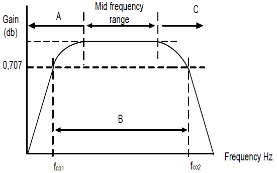
FIGURE 6.5: FREQUENCY RESPONSE CURVE OF A RC COUPLED AMPLIFIER.
6.5.1 Identify points A, B, and C. (3)
6.5.2 Describe how the voltage gain of an RC-coupled amplifier is affected at high frequencies. (3)
6.6 Refer to FIGURE 6.6 below and answer the questions that follow.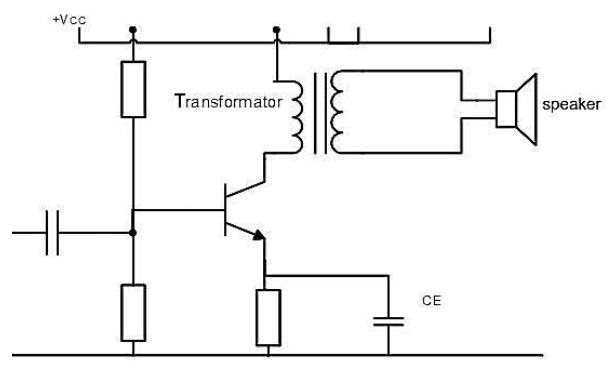
FIGURE 6.6: TRANSFORMER COUPLED AMPLIFIER
6.6.1 Describe the basic operation of the transformer coupled amplifier. (5)
6.6.2 State TWO advantages of a transformer coupled amplifier. (2)
6.7 With reference to a push-pull amplifier NPN transistor. Answer the questions that follow.
6.7.1 Explain how cross over distortion occurs. (2)
6.7.2 Calculate the current gain in dB by using the following information:
- Output power = 100 W
- Input power = 4 W
- Input voltage = 100 V
- Input current = 100 mA
- Output impedance = 20 Ω (6)
[45]
TOTAL: 200
FORMULA SHEET: