Electrical Technology: Electronics Memorandum - Grade 12 September 2021 Preparatory Exams
Share via Whatsapp Join our WhatsApp Group Join our Telegram GroupINSTRUCTIONS TO MARKERS
- All questions with multiple answers imply that any relevant, acceptable answer should be considered.
- Calculations:
2.1 All calculations must show the formulae.
2.2 Substitution of values must be done correctly.
2.3 All answers MUST contain the correct unit to be considered.
2.4 Alternative methods must be considered, provided that the correct answer is obtained.
2.5 Where an incorrect answer could be carried over to the next step, the first answer will be deemed incorrect. However, should the incorrect answer be carried over correctly, the marker has to re- calculate the values, using the incorrect answer from the first calculation. If correctly used, the candidate should receive the full marks for subsequent calculations.
2.6 Markers should consider that candidates' answers may deviate slightly from the marking a guideline depending on how and where in the calculation rounding off was used. - These marking guidelines are only a guide with model answers.
- Alternative interpretations must be considered and marked on merit. However, this principle should be applied consistently throughout the marking session at ALL marking centres.
MEMORANDUM
QUESTION 1: MULTIPLE CHOICE QUESTIONS
1.1
1.1 B (1)
1.2 A (1)
1.3 D (1)
1.4 C (1)
1.5 C (1)
1.6 A (1)
1.7 D (1)
1.8 A (1)
1.9 C (1)
1.10 D (1)
1.11 D (1)
1.12 A (1)
1.13 B (1)
1.14 D (1)
1.15 B (1) [15]
QUESTION 2: OCCUPATIONAL HEALTH AND SAFETY
2.1
2.1.1 The probability that injury or damage will occur. (1)
2.1.2 Free from any hazard. (1)
2.2
- In quantitative risk analysis, an attempt is made to numerically determine the probabilities of various adverse events and the likely extent of losses if a particular event took place.
- Qualitative risk analysis defines the various threats determining the extent of vulnerabilities and devising counter measures should a risk occur. (5)
2.3
- Use or misuse of power tools.
- Incorrect use and handling of hand tools.
- Etching of printed circuit boards. (Any 1 x 1) (1)
2.4 Inadequate lighting leads to poor visibility, which could lead to dangerous situations or injuries. (2)
[10]
QUESTION 3: RLC CIRCUITS
3.1 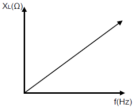
1 mark for correct labelling of axes
1 mark for correct shape of curve (2)
3.2 The capacitive reactance is inversely proportional to the frequency. (1)
3.3 It is the shift in phase between the supply voltage and the circuit current which results from the reactance and resistance in the circuit. (2)
3.4
3.4.1 The current lags the voltage. (1)
3.4.2 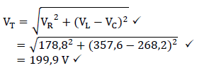 (3)
(3)
3.4.3 This occurs during resonance, when the voltage drop across the capacitor is equal to the voltage drop across the inductor. (2)
3.5 Used to tune radio and tv stations to a particular station. (1)
3.6
- In series current is maximum and in parallel current is zero.
- In series impedance is minimum and in parallel impedance is maximum. (2)
3.7
3.7.1
- X? = 2?ƒ?
= 2 × ? × 50 × 50 × 10−3
= 15,71 Ω (3)
3.7.2 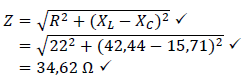 (3)
(3)
3.7.3
- XC = 1
2πfC
C = 1
2πfX?
= 1
2×π×50×42,44
= 7,5 × 10⁻⁵F
= 75 µF (4)
3.8
3.8.1
- XC = 1
2πfC
= 1
2×π×25×100×10−6
= 63,66 Ω - IC = V
X?
= 100
63,66
= 1,57 A (5)
3.8.2 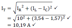 (3)
(3)
3.8.3  (3)
(3)
[35]
QUESTION 4: SEMICONDUCTOR DEVICES
4.1
- P-channel JFET or PFET
- N-channel JFET or NFET (2)
4.2
- Cut off region
- Negative resistance region
- Saturation region (3)
4.3 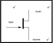 (3)
(3)
4.4
4.4.1 The emitter is a heavily doped p-type semi-conductor. (2)
4.4.2 The intrinsic standoff ratio is determined by the ratio of the internal resistances (rb1 to rb1 + rb2). (2)
4.4.3 The moment the emitter voltage (VE) is increased to above Vx the UJT is said to fire and goes into its trigger state. (2)
4.5 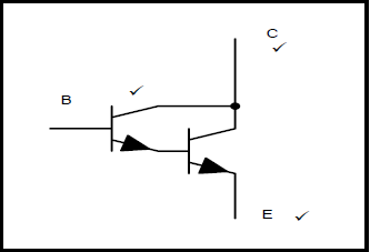 (3)
(3)
4.6
- The most important advantage of the Darlington pair as detailed above is its high current gain. This is decided by the gain of each individual transistor.
- Circuits improved input impedance ,this can be shown to be substantially increased making it far less likely to load any preceding stage of the circuit and so demand far less current to operate.
- When used in the common collector form the Darlington pair also develops very low output impedance. (4)
4.7
4.7.1
- 1 – non-inverting
- 2 – inverting (2)
4.7.2 It is important for the Op-amp to have a dual voltage supply to be able to amplify all signals above 0 V and below 0 V (positive and negative signals). (2)
4.8
- Differential Amplifier
- High Gain Differential Amplifier
- Common Collector (3)
4.9 Positive Supply (+V) (1)
4.10 The op-amp should be able to amplify any input of any frequency, from 0 Hz through to radio frequency and higher. This is not practical and the gain drops at higher frequencies. This is due to internal capacitances in the op-amp’s chip. (4)
4.11
- Very high input impedance
- Very low output impedance (2)
4.12 This pin is used to allow a different charge voltage level to be introduced to the 555 timer rather than the usual 2/3 point. This pin is normally either not connected or else it is connected to ground via a small value capacitor which removes any unwanted noise from the supply voltage that might affect the timer operation. (4)
4.13 This capacitor will remove any unwanted noise from the supply voltage which could affect the operation of the timer. (2)
4.14
- Two comparators
- S/R flip-flop (2)
4.15
- Monostable
- Astable
- Bistable (Any 2 x 1) (2)
[45]
QUESTION 5: SWITCHING CIRCUITS
5.1
5.1.1 Bistable multivibrator (1)
5.1.2 It protects the LED from drawing to much current and getting damaged. (1)
5.1.3 When RESET is pressed, Pin 4 is pulled to ground. This resets the IC and cause it to change state with the output falling to LOW. (3)
5.1.4 The low value capacitor (0,1µF) is used to remove any unwanted and stray signal from the circuit. The will prevent noise in the circuit. (3)
5.1.5
- The two inputs would be floating between +V and 0 V.
- When the SET or RESET button is pushed it would short circuit the supply to ground. (2)
5.2 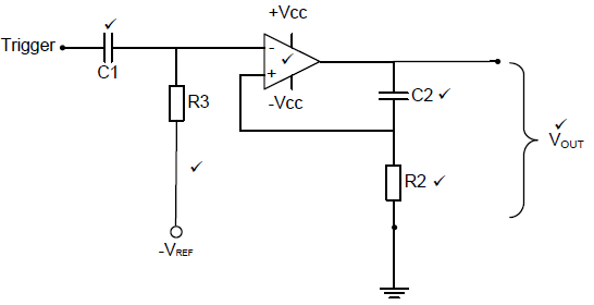 (6)
(6)
5.3
- Change the value of the timing capacitor.
- Change the value of the timing resistor.
- Change the values of both the timing capacitor and the timing resistor. (3)
5.4 Switch bounce can be eliminated by using a monostable multivibrator circuit to control the output. (1)
5.5 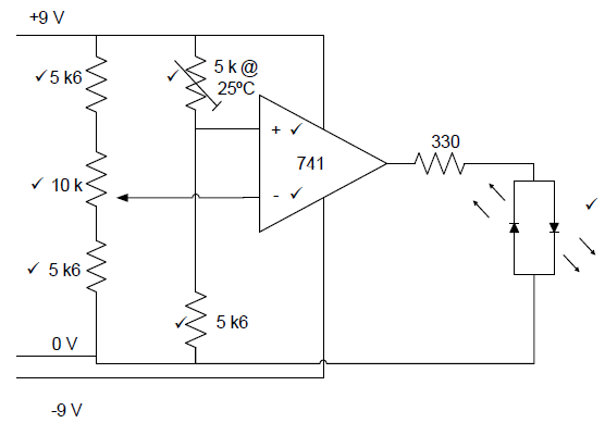 (8)
(8)
5.6
- The less light on the LDR, the higher the resistance.
- The more light on the LDR, the lower the resistance. (4)
5.7
5.7.1 Open loop gain refers to a circuit with no feedback from the output back to the input. (2)
5.7.2
- Voltage divider resistors R1 and R2 set up the reference voltage VREF.
- The reference voltage is fed back to the non-inverting input of the op-amp.
- The comparator compares the input voltage VIN to the reference voltage VREF.
- The gain of the op-amp is ±100 000 because of the open loop connection.
- Whenever there is a fraction of a millivolt difference between VIN and VREF, this difference will be amplified.
- The op-amp will be driven into either one of the saturation states. (6)
5.8
5.8.1 By adding another input resistor to the summing amplifier input. (1)
5.8.2 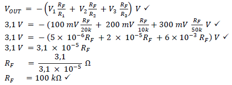 (4)
(4)
5.8.3 It is negative because the inputs are fed into the inverting input, which will cause the output to be 180° out of phase. (1)
5.9 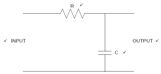 (4)
(4)
[50]
QUESTION 6: AMPLIFIERS
6.1
6.1.1
- To set the operating conditions (points) of the transistor.
- To stabilise the operating point of the transistor. (2)
6.1.2 Q-point on the DC load line represents the voltages across the transistor. and current through the transistor when no input signal is applied. (2)
6.1.3 Vce = Vcc (1)
6.1.4
- ?? = ???
??
= 9 ?
800 Ω
= 11,25 ? (3)
6.1.5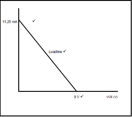 (3)
(3)
6.2
- ?1 = 20 ??? ????
?i?
= 20 ???10 15,3×10⁻³
3,6×10⁻³
?? = 12,57 ?? (3)
6.3
- Improving the amplifiers stability.
- Increase the amplifiers bandwidth.
- Enhancing the amplifiers input and output impedances
- Reducing or suppressing a noise produced within the amplifier. (Any 2 x 1) (2)
6.4
6.4.1
- When an AC voltage is applied to the input of the first amplifier stage, an alternating current will flow in the collector circuit of transistor.
- An alternating voltage will develop across the collector resistor (RC1). The developed alternating voltage across the RC1 will be transferred through capacitor C2 to the base of the transistor (Q2) in the amplifier’s second stage (stage 2).
- The process will be repeated and the amplified output will measured between C3 and 0 V. (6)
6.4.2
- Cheap, economical and compact as it uses only resistors and capacitors.
- Offers a constant gain over a wide frequency band. (2)
6.5
6.5.1
- A – Low frequency range
- B – Bandwidth
- C – High frequency range (3)
6.5.2 At the higher frequency as the signal frequency rises it encounters small parasitic capacitances which develop inside of the transistors. These capacitances appear between the different regions of the transistor due to their different biasing voltages as the signal frequency rises. The effect of these capacitor increases, with their reactance become lower and lower. (3)
6.6
6.6.1
- Transformer coupled amplifiers are made from coils of copper wire.
- The transformer winding resistance is very low.
- When used as the collector load in a transistor amplifier this creates a very high current with a small voltage output.
- This is useful for driving low impedance loads such as relays, loudspeakers and motors. (5)
6.6.2
- Excellent impedance matching can be achieved.
- Total DC isolation between stages. (2)
6.7
6.7.1
- When the DC base voltage drops to zero, transistors are OFF.
- The input signal must pass through the region where both transistors are not conducting. (2)
6.7.2 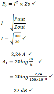 (6)
(6)
[45]
TOTAL: 200